עוד בפרק זה:
Atom Force Microscopy Laboratory
Head of the Laboratory: Dr. Igor Lapsker
Tel: 972-3-5026609
Fax: 972-3-5026619
Fax: 972-3-5026619
Atom Force Microscopy Laboratory supports a research programs on the analysis and characterization of fullerenes, thin films, coatings and bulk materials.
We work in fields of microelectronics, micromechanical electronic systems, trybology and nanotrybology, superconductivity, medicine materials and plasma applications to materials treatment.
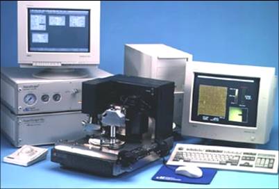
Fig. 1. The Atom Probe Microscope
The Dimension 3100 Scanning Probe Microscope (SPM) utilizes automated atomic force microscopy (AFM) and scanning tunneling microscopy (STM) techniques to measure surface characteristics for semiconductors wafers, lithography masks, magnetic media, CDs/DVDs, biomaterials, optics, and other samples up to 200mm in diameter.
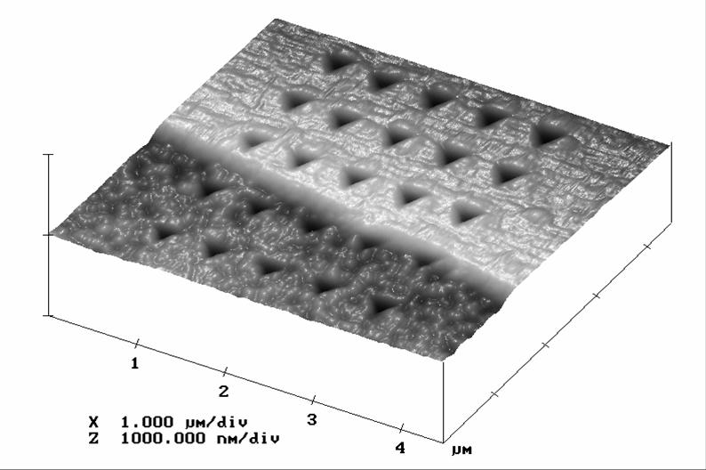
Fig. 2. Atom Force Microscope image of the array of nanoindents in two neighboring grains in polycrystalline cooper of very high purity.
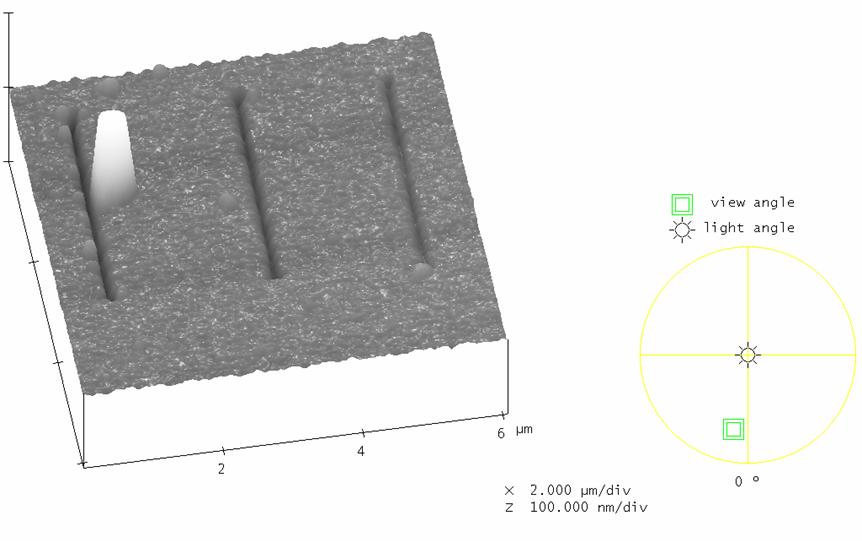
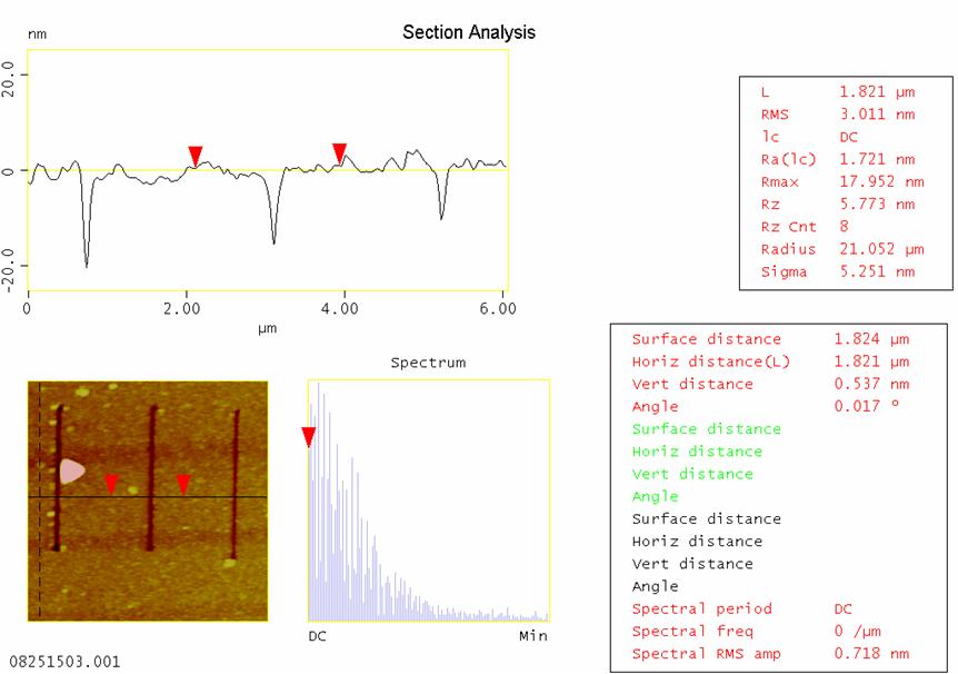
Fig. 3. Scratches produced on the surface by microindentor (a)
and section analysis (b)
and section analysis (b)
- כתבות, חדשות ואירועים


